My History with Mainframes
by: Paul Bishop
I started working on IBM mainframes at the end of 1980, just after graduating from high-school.
First job was to assist Richard Kader from Circle Computer Services (Schaumburg, IL) with the de-install of a 3148 and installation of a 3158 in Hackensack, NJ.
I don't remember the name of the bank.
For the next few years I worked full-time for Circle with installs, de-installs, upgrades, etc., of various machines; 3158, 3168, 3033, 3031, 3032.
Most of my work was on the 3033.
Lots of installs and feature work like data-streaming (104x), director 3 installs (channels 13-16 / frame 07), memory upgrades, channel-to-channel adapters, etc.
Did a lot of jobs with my brother Glenn who taught me everything I know.
In 1984 I quit Circle to become independent.
I continued to work on 3033 and slowly switched to 308X (3081, 3083, 3084) as they became popular.
In 1987 I designed memory for the 308X series and in 1988 I started BSM Corporation (Schaumburg, IL) with my brother and father (Glenn and Glenham respectively) to design and manufacture memory for IBM mainframes.
I continued to design and manufacture memory for 308X, 3090, and 9121 machines through the end of 1994.
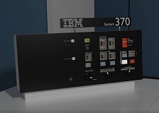
IBM 3033
The 3033 was my favorite machine because it was the last machine you could actually scope, diagnose, and fix.
The 308X series introduced the TCM and you really never needed to carry around a scope after that (maybe to diagnose power problems).
My conjecture is that there were two mainframe teams at IBM: 3033 > 3090 > ES-9000 and 4381 > 308X > 9121.
Not sure, but that's how the machines smelled.
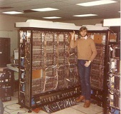
- 1: Me and a 3033 (circa 1981). Frame 02 (IPPF, E-FUNC) to my right, Frame 01 (PSCF, Trace, Clocks) to my left. High-speed multiple board (A2) under my elbow. A $hit-long time ago.
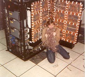
- 2: They didn't pay us much so we had to eat whatever was laying around. Snacking on some 50Ω(purple) & 90Ω(orange) tri-leads between the gates of director 2 (frame 05).
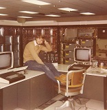
- 3: Sitting on the 3036 console. Frame 01 background left (silver covers). Frame 03 (memory) background center. Frame 04 (power supplies) background right.
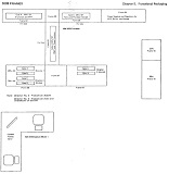
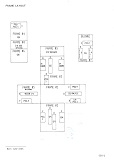
- 4: 3033 Uniprocessor Frame Layout


My 3033 3D Model Fly-Around Video. Yeah I need to work on the 3277s and grills for the 3036 doors (and panel). I'm a new blender user - so give me a pass on this one.

IBM 4331
I purchased a 4331 (the only S/370 mainframe that ran on single-phase 240v) to repair memory cards for 4331, 4341and 4361 machines.
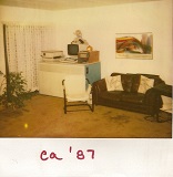
- Below Left: 4331 in my apartment, circa 1987
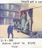
- Right: Moving that 4331 to BSM, 1988. My brother Glenn (upper left), my brother Tom (upper right), and my father.


Note: IBM hierarchy/terminology is Card > Board > Gate > Frame, so memory cards plug into boards, boards are in gates, gates are in frames.
BSM 308X Memory
In 1987 I designed memory for the IBM 308X series mainframes.
Microcode was on 8" floppy which contained the machine configuration.
I purchased an 8" drive system, analyzed the disk layout, analyzed the configurations, and wrote two assembly (x86) programs; PDU and PCF.
PDU (Processor Disk Utility) was a utility that allowed you to view and alter diskette contents.
PCF (Processor Configuration Facility) was a utility that displayed the existing machine configuration and allowed the user to alter the config, e.g. set memory size, add channels, etc.
Sold several PDU/PCF systems to various staging houses (Comdisco, Circle, Enterprise, Data Hardware, etc.).
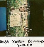
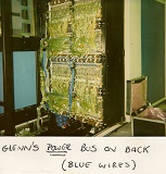
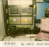
- Below Left: 1st 308X protype working on the backplane (IBM card unplugged from the front). Circa 1987. Green tri-leads are 80Ω (data lines had 80Ω resistor on each end).
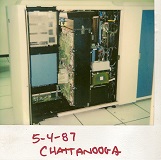
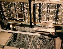
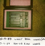
- Center: 308X Frame S Memory gate backplane and 8 boards (this was a 3083 at Computer Express in Chattanooga). Circa 1987.
- Right: 308X Frame S Memory gate side view.


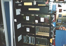
- 1: 308X Frame S Memory gate front view (card slots).
- 2: Another view of 308X Frame S with memory gate.
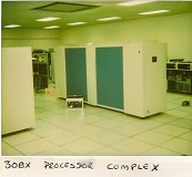
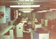
- 3: 308X Frame S (left), frame X (center), and frame F (right end). Extreme left is the service processor and console frame.
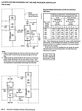
- 4: 308X Frame Layout


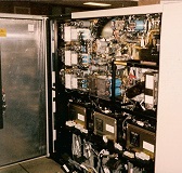
- Below Left: Showing the other side of frame S with one CPU (left) and the channel controller (right).
Another CPU is above left and the system controller is above right (not shown).
This picture was from a 3081 install at TRW in Anaheim, circa APR-1985.
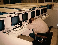
- Center Left: Catching some Zs on that job with 3350 farm in the background.
- Center Right: Inside the service processor frame (channel drivers bottom, channel power supplies top-left, service processor HDD right).
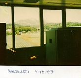
- Right: Threw in a nice picture of a 3081 next to a vinyard in Marsalles, Frace, circa 1987. Don't remember what the job was. Channels I think.
- Far Right: Yeah, super crappy pic but 1st time on a Concorde (OK, the only time - but who's asking?).


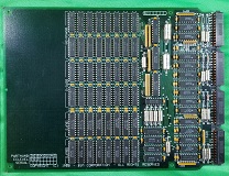
BSM 308X cards used 64K x 4 DRAM (1MB) card. 18 cards in board. Max 8 boards in the frame.
Each card was 4 bits wide by 8 buffers deep. Two boards next to each other make up a bus (144 bits wide). Two separate busses as you can see from the above photos.
For example, the bottom 4 boards worked as one array while the upper 4 boards worked as another. Vertically two of the four boards shared the same data bus.
As I mentioned, memory was 8 buffers deeps so the CPU would write/read 144bits x 8deep (1152 bits) in one storage cycle.
The BSM card was double the highest IBM card density so we only needed to populate 2 boards of a set to max out storage.
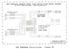
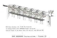
We needed the 308X quad card (went on the back of each of 2 boards) to merge some control signals from the upper board pair.
Lots of ECL here because the bus was current mode terminated to ground with 80ohm resistors and pulled down to ~-1V when driven.
Basically the current switch side of an ECL differential pair (before the output driver), hence the 10192s.
We paired 2x 10192 gates for the drive current and tied the other side of the emitter pair to ground to force the current to switch as quickly as possible.
Power was +5V for the DRAM and -4.25V for the logic. The 10K ECL ran fine @ -4.25V for this application.
There was a -5V supply present in the memory boards but this was low power for bias so we stole the high-current -4.25V from the CPU board. They had plenty-o-current (-4.25V @ 1200A!).
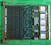
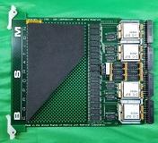
- 1: Early 308X beta card. Company name came from the IBM acronym for Basic Storage Module. Better name would have been HAL.
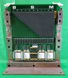
- 2: Later 308X production card.
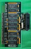
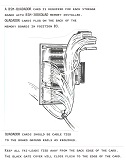
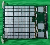
- 3: 308XQUAD Control-Line Merge Card (created another address line depending on whether the top or bottom board signals were active).
- 4: 308XQUAD installation drawing.
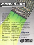
- 5: BSM 308X Sell-Sheet


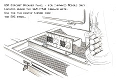
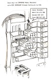
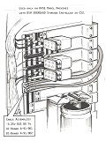
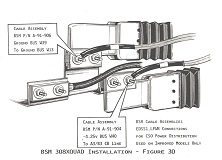
Various BSM 308X Installation drawings by my brother Tom.


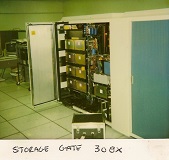
Left: 2x 3083s on the staging floor and one on the dock. Right: 308X Storage Gate for Live Machine Testing before customer install.


BSM 3090 Memory
The 3090 had both 'Main' and 'Expanded' storage.
Main storage was 2x boards in frame 01, gate F. Each card had 4bits x 16 buffers deep.
Expanded storage was 4x boards in Frame 02, gate C.
Each board held 18 memory cards, plus address line drivers and terminator cards (20 cards total per board).
The 3090 Service Processor ran VM itself and the machine configuration came on tape.
The machine configuration was in a file called PRISTINE.MCT and naturally we wrote a program to analyze and modify called FU2 (File Utility, version 2).
- 1: Main storage 'PIG8' card (8MB-piggy-back onto IBM card). 36 Cards in two boards in the main storage gate, PMAX and PMAY.
- 2: Main storage 'Antelope' card using IBM control chips. Foam was to guide air flow.
- 3: Main storage card in a soldering fixture.
- 4: Expanded storage card. 72 cards in 4 boards in the expanded storage gate.
- 5: 3090 Frame Layout. Main storage (PMAX/PMAY) 2 boards (36 memory cards) in Frame 01 Gate F - Max 512MB. Expanded storage (ESA) 4 boards (72 cards) in Frame 02 gate C - Max 1024MB).


BSM 3090 Media (from left to right):
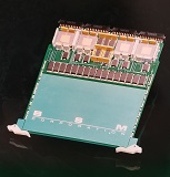
- 1: Main Storage Product Shot
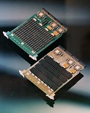
- 2: Expanded Storage Product Shot
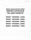
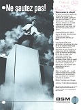
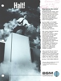
- 3: Sell Sheet
- 4: Brochure (English)
- 5: Brochure (French)
- 6: Brochure (German)
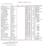
- 7: BSM 3090 Customer Install List


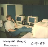
Doing some 3090 job in Frankfurt:

BSM 9121 Memory
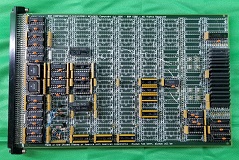
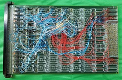
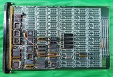
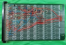
The 9121 had 8 cards in a board with 18 bits each. We used a lot of 10K and 100K ECL for the prototypes and a custom ECL chip in production.
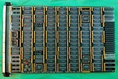
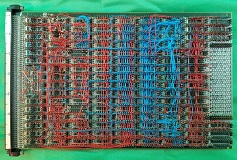
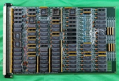
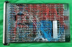
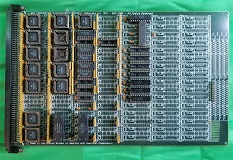
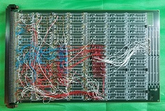
BSM 9121 Prototypes. Below are the fronts and backs of various prototyping cards.
Naturally we needed to design and produce the raw prototyping circuit boards before we could create the prototypes.
I think these were 8-layer boards with two ground planes and 4 voltage planes.
Signals were ~+/-500mv around ground.
Power was +2.8V, +1.4V, GND, -0.7V, and -2.2V.
5V DRAM was powered across +2.8V and -2.2V.
3.6V ECL-like logic powered by +1.4V and -2.2V with 0.7V for terminators.
 |
 |
This whole prototype card only handled 3 of the 18 production card bits - so 3 times this logic went into one of the custom production chips (2 per card). |
 |
 |
 |
 |
Looks like we were checking the custom production BSM9000A chip (wired upside-down on back side). |
 |
 |
No clue what that chip is in the back. I think we we're checking some existing driver to see if it would work for this application. |
 |
 |
BSM 9121 Production cards
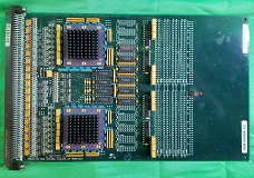
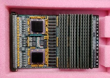
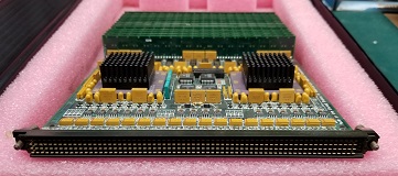
- Below Left: Pre-Production card (without memory sticks).
- Center: Production card (almost full). Large custom ECL chips are marked BSM9000A.
- Right: 67 x 4 pins. That's a fun connector. Trust me.


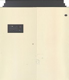
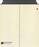
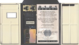
BSM 9121 Brochure - Fold out that looked like a 9121 (from left to right):
- 1: 9121 Brochure Front
- 2: 9121 Brochure Back
- 3: 9121 Brochure Inside - Single 8 slot memory board where the BSM9000A label is.


BCC 9121 Memory
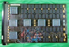
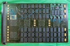
I designed a 9121 mezzanine module for my brother's company, Bishop Computer Corp.
IBM used custom memory chips so the Xilinx XL9536 PGA converted the IBM custom DRAM signals for use with regular memory.
This solution worked but was cumbersome and never put into production.
The mezzanine module you see in the 2nd pic replaced IBM DRAM chips on both sides of the board.
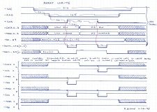
The IBM chips had this funky aligned-write buffering when you could write bits starting at any of 4 addresses. Strange stuff to replicate.
- 1: Prototyping the logic.
- 2: Testing the production mezanine module.
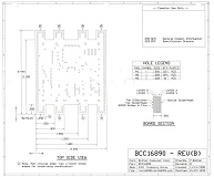
- 3: PCB Manufacturing Notes
- 4: Sample timing diagram notes.


BSM Marketing
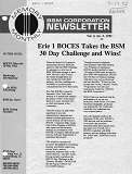
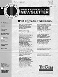
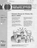
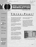
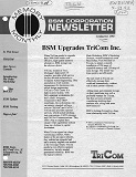
We created some newsletters in 1991 and 1992.
They were separated for end-users and brokers so there is some duplication.
The numbering convention was all over the place so these are mixed up a bit - hover to see the publication info.
These sported the "Memory Man" cartoon series drawn by my brother Tom.
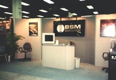
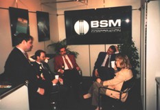
Trade Shows - Left in Chicago, Right @ Hannover Mesa


Updated 2022-02-09
